- 您现在的位置:买卖IC网 > Sheet目录2008 > MAX1202AEPP+ (Maxim Integrated Products)IC ADC 12BIT 8CH 20-DIP
MAX1202/MAX1203
5V, 8-Channel, Serial, 12-Bit ADCs
with 3V Digital Interface
_______________________________________________________________________________________
9
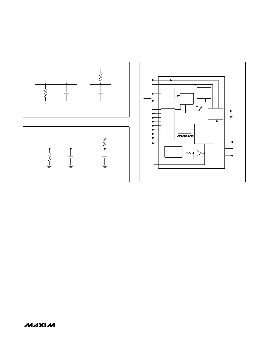
_______________Detailed Description
The MAX1202/MAX1203 analog-to-digital converters
(ADCs) use a successive-approximation conversion
technique and input track/hold (T/H) circuitry to convert
an analog signal to a 12-bit digital output. A flexible ser-
ial interface provides easy interface to 3V microproces-
sors (Ps). Figure 3 is the MAX1202/MAX1203 block
diagram.
Pseudo-Differential Input
Figure 4 shows the ADC’s analog comparator’s sam-
pling architecture. In single-ended mode, IN+ is inter-
nally switched to CH0–CH7 and IN- is switched to
GND. In differential mode, IN+ and IN- are selected
from pairs of CH0/CH1, CH2/CH3, CH4/CH5, and
CH6/CH7. Configure the channels using Tables 3
and 4.
In differential mode, IN- and IN+ are internally switched
to either of the analog inputs. This configuration is
pseudo-differential such that only the signal at IN+ is
sampled. The return side (IN-) must remain stable (typi-
cally within ±0.5LSB, within ±0.1LSB for best results)
with respect to GND during a conversion. To do this,
connect a 0.1F capacitor from IN- (of the selected
analog input) to GND.
During the acquisition interval, the channel selected as
the positive input (IN+) charges capacitor CHOLD. The
acquisition interval spans three SCLK cycles and ends
on the falling SCLK edge after the input control word’s
last bit is entered. The T/H switch opens at the end of
the acquisition interval, retaining charge on CHOLD as a
sample of the signal at IN+.
The conversion interval begins with the input multiplex-
er switching CHOLD from the positive input (IN+) to the
negative input (IN-). In single-ended mode, IN- is sim-
ply GND. This unbalances node ZERO at the compara-
tor’s input. The capacitive DAC adjusts during the
remainder of the conversion cycle to restore node
ZERO to 0V within the limits of 12-bit resolution.
This action is equivalent to transferring a charge of
16pF x [(VIN+) - (VIN-)] from CHOLD to the binary-
weighted capacitive DAC, which in turn forms a digital
representation of the analog input signal.
Figure 1. Load Circuits for Enable Time
Figure 2. Load Circuits for Disable Time
Figure 3. Block Diagram
+3.3V
3k
CLOAD
GND
DOUT
CLOAD
GND
3k
DOUT
a. High-Z to VOH and VOL to VOH
b. High-Z to VOL and VOH to VOL
+3.3V
3k
CLOAD
GND
DOUT
CLOAD
GND
3k
DOUT
a. VOH to High-Z
b. VOL to High-Z
INPUT
SHIFT
REGISTER
CONTROL
LOGIC
INT
CLOCK
OUTPUT
SHIFT
REGISTER
+2.44V
REFERENCE
T/H
ANALOG
INPUT
MUX
12-BIT
SAR
ADC
IN
DOUT
SSTRB
VDD
VL
VSS
SCLK
DIN
CH0
CH1
CH3
CH2
CH7
CH6
CH5
CH4
GND
REFADJ
REF
OUT
REF
CLOCK
+4.096V
20k
≈ 1.68
1
2
3
4
5
6
7
8
10
11
12
13
15
16
17
18
19
MAX1202
MAX1203
(MAX1202)
CS
SHDN
A
20
14
9
发布紧急采购,3分钟左右您将得到回复。
相关PDF资料
MAX121EAP+
IC ADC 14BIT 308KSPS 20SSOP
MAX1238MEEE+T
IC ADC 12BIT SERIAL 16-QSOP
MAX1240AEPA+
IC ADC 12BIT SERIAL 8-DIP
MAX1245BCPP
IC ADC SRL 12BIT 2.375V 20-DIP
MAX1249AEPE+
IC ADC 10BIT SERIAL 16-DIP
MAX1279AETC+
IC ADC 12BIT 1.5MSPS 12-TQFN
MAX1285BESA+T
IC ADC 12BIT 300KSPS 8-SOIC
MAX1302BEUG+
IC ADC 16BIT SRL 115KSPS 24TSSOP
相关代理商/技术参数
MAX1202BC/D
功能描述:模数转换器 - ADC RoHS:否 制造商:Texas Instruments 通道数量:2 结构:Sigma-Delta 转换速率:125 SPs to 8 KSPs 分辨率:24 bit 输入类型:Differential 信噪比:107 dB 接口类型:SPI 工作电源电压:1.7 V to 3.6 V, 2.7 V to 5.25 V 最大工作温度:+ 85 C 安装风格:SMD/SMT 封装 / 箱体:VQFN-32
MAX1202BCAP
功能描述:模数转换器 - ADC Integrated Circuits (ICs) RoHS:否 制造商:Texas Instruments 通道数量:2 结构:Sigma-Delta 转换速率:125 SPs to 8 KSPs 分辨率:24 bit 输入类型:Differential 信噪比:107 dB 接口类型:SPI 工作电源电压:1.7 V to 3.6 V, 2.7 V to 5.25 V 最大工作温度:+ 85 C 安装风格:SMD/SMT 封装 / 箱体:VQFN-32
MAX1202BCAP+
功能描述:模数转换器 - ADC 12-Bit 8Ch 133ksps 5V Precision ADC RoHS:否 制造商:Texas Instruments 通道数量:2 结构:Sigma-Delta 转换速率:125 SPs to 8 KSPs 分辨率:24 bit 输入类型:Differential 信噪比:107 dB 接口类型:SPI 工作电源电压:1.7 V to 3.6 V, 2.7 V to 5.25 V 最大工作温度:+ 85 C 安装风格:SMD/SMT 封装 / 箱体:VQFN-32
MAX1202BCAP+T
功能描述:模数转换器 - ADC 12-Bit 8Ch 133ksps 5V Precision ADC RoHS:否 制造商:Texas Instruments 通道数量:2 结构:Sigma-Delta 转换速率:125 SPs to 8 KSPs 分辨率:24 bit 输入类型:Differential 信噪比:107 dB 接口类型:SPI 工作电源电压:1.7 V to 3.6 V, 2.7 V to 5.25 V 最大工作温度:+ 85 C 安装风格:SMD/SMT 封装 / 箱体:VQFN-32
MAX1202BCAP-T
功能描述:模数转换器 - ADC RoHS:否 制造商:Texas Instruments 通道数量:2 结构:Sigma-Delta 转换速率:125 SPs to 8 KSPs 分辨率:24 bit 输入类型:Differential 信噪比:107 dB 接口类型:SPI 工作电源电压:1.7 V to 3.6 V, 2.7 V to 5.25 V 最大工作温度:+ 85 C 安装风格:SMD/SMT 封装 / 箱体:VQFN-32
MAX1202BCPP
功能描述:模数转换器 - ADC RoHS:否 制造商:Texas Instruments 通道数量:2 结构:Sigma-Delta 转换速率:125 SPs to 8 KSPs 分辨率:24 bit 输入类型:Differential 信噪比:107 dB 接口类型:SPI 工作电源电压:1.7 V to 3.6 V, 2.7 V to 5.25 V 最大工作温度:+ 85 C 安装风格:SMD/SMT 封装 / 箱体:VQFN-32
MAX1202BCPP+
功能描述:模数转换器 - ADC 12-Bit 8Ch 133ksps 5V Precision ADC RoHS:否 制造商:Texas Instruments 通道数量:2 结构:Sigma-Delta 转换速率:125 SPs to 8 KSPs 分辨率:24 bit 输入类型:Differential 信噪比:107 dB 接口类型:SPI 工作电源电压:1.7 V to 3.6 V, 2.7 V to 5.25 V 最大工作温度:+ 85 C 安装风格:SMD/SMT 封装 / 箱体:VQFN-32
MAX1202BEAP
功能描述:模数转换器 - ADC RoHS:否 制造商:Texas Instruments 通道数量:2 结构:Sigma-Delta 转换速率:125 SPs to 8 KSPs 分辨率:24 bit 输入类型:Differential 信噪比:107 dB 接口类型:SPI 工作电源电压:1.7 V to 3.6 V, 2.7 V to 5.25 V 最大工作温度:+ 85 C 安装风格:SMD/SMT 封装 / 箱体:VQFN-32